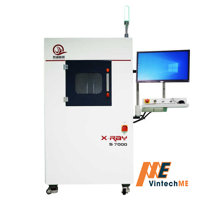
Electronics X-ray Inspection | HT100
Introducing our another cutting-edge inspection system designed to detect welding defects in electronic components, providing unparalleled accuracy and reliability for quality assurance.
Our advanced detection system is designed specifically to identify welding defects in electronic components, ensuring high-quality standards for various applications.
Experience the precision and reliability of our X-ray detection system, designed for use in semiconductor, SMT, DIP, and various electronic component inspections, including IC, BGA, CSP, and flip chips.
Our advanced X-ray detection system is engineered for semiconductor, SMT, DIP, and a variety of electronic components, including ICs, BGA, CSP, and flip chips, delivering unparalleled precision and efficiency.
Discover our high-performance inspection system, designed to meet universal inspection requirements with a strong penetrating ray source and HD FPD, ensuring comprehensive and accurate detection for various applications.
Our advanced inspection equipment is specifically designed for detecting BGA and chip components, nickel plate detection on metal plates, and FPC welding parts. It efficiently calculates bubble percentages, measures size and area, and analyzes internal defects such as low tin and virtual soldering in products.