


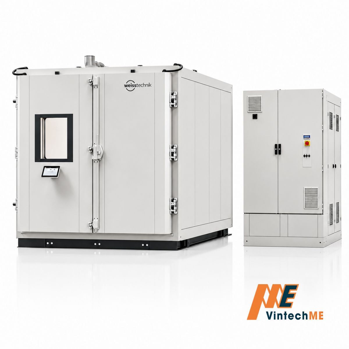
Overview
The MirXT-160 is a cutting-edge 3D X-ray inspection system tailored for advanced wafer technology, SMT, packaging inspection, semiconductor, and laboratory applications. It excels in detecting solder/tin voids and bonding wire issues commonly found in the SMT and semiconductor manufacturing processes within the electronics industry. The system effectively identifies packaging defects such as offsets, wire cross short circuits, flip-chip solder ball issues, wire breakage, and detachment.
Functions and Features
- Modular design, user-customized system
- Multi-axis motion control system enables clear detection from different angles
- Automatic real-time navigation chart and X-ray image navigation chart function
- Specially designed OVHM module, the detector can rotate 360 degrees horizontally and tilt 70 degrees
- Ultra-high-speed, high-definition CT images
- Product process programming, with automatic detection function, 5-axis interpolation function, visual CNC detection, and unlimited point editing
- Digital real-time image processing technology, professional configuration HDR image enhancement technology functions
- Maximum tube voltage: 160KV, maximum power 20W
- Geometric magnification up to 2100x, total magnification up to 23000x
- The smallest detection capability can reach: 0.35 micron
- OVHM technology for high magnification bevel detection
Detailed Specifications
|
System Magnification and Resolution |
|
|
Geometry Magnification Time |
2100x |
|
Total Magnification |
>23000X |
|
Details Resolution |
Up to 0.35 microns |
|
Submicron X-ray Tube |
Open micron tube, transmission tube head, 170 °radiation Angle, collimation function |
|
Maximum Tube Voltage |
160KV |
|
Maximum Power |
20W |
|
Target |
Non-toxic carrier tungsten target and can be rotated for multiple uses |
|
Vacuum System |
Oil-free low vacuum pump + turbo molecular vacuum pump |
|
Detector |
1536*1536pixel |
|
Control Platform |
X-ray automatic navigation system, can achieve internal and external navigation |
|
Overall Structure |
High precision anti-vibration, 5-axis synchronous drive |
|
Maximum Detection Range |
410mm×410mm |
|
Maximum Work piece Size/Weight |
510mm×510mm/5kg |
|
Probe WNW Triangle View Rotated |
Adjustable viewing Angle 70°,n×360° |
|
Control |
Joystick control or mouse (manual mode) CNC programming Control(automatic mode) |
|
Control AIDS |
X-ray image navigation map, click to move function, click to enlarge function, Automatically maintain the center of vision function, laser positioning and aiming |
|
Anti-Collision System |
Prevent the test sample from colliding with the ray tube |
|
Image processing software |
|
|
ELT x/act base |
Comprehensive X-ray image analysis software includes image contrast enhancement and filtering. measurement, CNC programming |
|
BGA mode |
BGA solder joint automatic detection function |
|
VC mode |
Automatic calculation of void area ratio, including multi-chip mounting void detection function |
|
System scale (WxHD) |
1650mm*1680mm*1955mm (Excluding console and detachable rear extension) |
|
Console Height Adjustable |
320mm |
|
Maximum Weight |
About 3050kg |
|
Radiation safety protection |
Safety shielding room with lead steel protective structure and lead glass Windows, in accordance with German and American safety design standards for X-ray equipment |
|
Radiation leakage dose rate |
<1.0m Sv/h, in line with international standard |
|
Hardware options |
|
|
Tilt/rotate gear |
Tilt 70° and rotate n × 360* with a maximum workpiece weight of 5kg |
|
Laser posting device |
Cross laser wire |
|
Square non-rotiatng platform |
Test area to 510mm x 510mm |


 Tiếng Việt
 English